
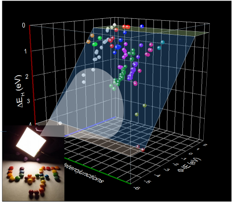
The general energy map (GEM) was created for charting interface energy levels over three distinct regions covering various material systems used in organic electronics. Here, the highest occupied molecular orbital binding energies (ΔEH) are plotted against the difference between the ionization energy and work function (ϕ-IE) at dozens of organic interfaces investigated for OLED (inset) applications. (Credit: Organic Optoelectronics Research Group)
April 25, 2017
Materials selection for organic thin-films in semiconductor and optoelectronic devices has traditionally been done by trial and error. Researchers and industry would have to experimentally test thin-film functionality and efficiency for use in devices such as organic light emitting diodes (OLEDs) and organic photovoltaics (OPVs). Now, MSE Professor Zheng-Hong Lu and MSE doctoral candidates Yiying Li and Peicheng Li have created a master map that will accelerate materials selection and guide organic device design.
Researchers and industry can refer to the map, which was published today in Advanced Materials, as a master guide in the selection of organic thin-film materials for fabricating organic optoelectronics.
As an example, OLEDs, the lighting technology that’s behind curved televisions and high-end smartphone displays, typically consist of a stack of several organic thin-films sandwiched between inorganic electrodes. The materials chosen as the organic thin-films contribute majorly to the device’s overall performance.
PhD candidate Yiying Li explains that while there are many factors that must be considered when designing such devices, the energy level alignment between thin-films deserves major attention. “When designing OLEDs or OPVs, one of the most important parameters is the energy level alignment at the interface of two different types of organic thin-films,” Li says. “The goal is to minimize the energy barrier at this interface to increase device efficiency.”
This molecular energy level alignment dictates how much power is required to move charges across molecules at the organic thin-film interface and the energy conversion efficiency of these charges to emit light.
The team conducted extensive research on several dozens of organic thin-film stacks and constructed energy level diagrams with data collected from ultraviolet photoemission spectroscopy.
“Right now, the community assumes a vacuum level alignment,” explains Li. “So basically, when the two thin-films are in contact with each other we assume there are no interactions happening at the interface. We found that this is not always the case — there may be interactions like charge transfer and other things happening.” These interactions revealed a general scientific principle that governs the molecular interface energy levels.
When asked why the optoelectronics community hasn’t already created a guide that seems so fundamental to organic device design, Professor Zheng-Hong Lu explains that many researchers have reported on certain combinations of thin-films, but have not sampled data to this scope.
“For example, researchers have studied single trees in a forest”, says Professor Lu. “We’ve looked at many different trees to tell the story of the entire forest.”
“This master map will help the community tremendously,” Professor Lu explains. “It will accelerate the development of new technologies so we can engineer the next generation of high performance devices.”
This work is a major milestone built on Professor Lu’s previous discovery of a universal energy alignment of molecules on metal oxides.