Newest innovation from OTI Lumionics enables integration of displays with different types of sensors and cameras, allowing device makers to create notch-free screens

OTI Lumionics, a Toronto-based company that spun out of research from U of T Engineering’s Department of Materials Science & Engineering, recently raised more than $75 million CAD in series B funding. The support will enable the company to further expand its line of organic LED technology solutions — including screens that are uninterrupted by the “notches” commonly found in today’s displays.
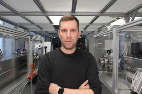
Founder and alumnus Michael Helander (MSE PhD 1T2) first realized the potential opportunity to commercialize his research after being approached by brand-name consumer-electronics companies during his PhD. Those companies were interested in the new materials and process technology he was developing for the manufacture of organic electronics.
Encouraged by his thesis supervisor, Professor Zhen-Hong Lu (MSE), Helander decided to license the technology and start a company in 2011. Since then, OTI’s technology focus has changed from applications such as consumer lighting to advanced displays, including organic LED (OLED). The company works with some of the largest consumer device brands in the world.
Helander believes that developing new materials represents the most “elegant” way to solve problems in manufacturing.
“Materials science and engineering is the foundation for all of electronics and most other major industries,” he says.
“When you drill down to the bottom of what enables it, it’s all about new materials. New software like AI and machine learning is only made possible by better chips, better storage, better hardware — and that better hardware is all enabled by new advanced materials that allow for more components such as transistors in a smaller and lower-energy package.”
OTI’s latest innovation is known as CPM Patterning and represents a new way to pattern print thin films, usually on the order of nanometres or micrometres in thickness. This is important because some of the techniques that have been developed over the last several decades, such as photolithographic patterning and laser ablation, can’t be used in certain manufacturing environments because the materials used are very sensitive to oxygen, moisture or other factors that are difficult to control.
“What we’ve done is come up with a process instead of new materials that allows you to pattern thin films, but instead of making a film and removing materials, you can grow a pattern from the ground up at the atomic level — it’s a 100% material- science-driven solution,” says Helander.
“What that lets manufacturers do in displays, for example, is pattern thin film coatings in the display that otherwise they couldn’t pattern before. That means they can start introducing new features and functionality that weren’t possible before, because they couldn’t be manufactured.”
One potential application of this innovation is integration of displays with different types of sensors and cameras. For example, the dark spaces or “notches” that we see on our smartphones, tablets and laptops are necessary to give space for the front facing camera.
“The idea is, if you can pattern, little, tiny holes in the display between all the pixels, then those cameras and sensors can be integrated under the display. You don’t have any kind of black area that doesn’t function, so you can get more usable display without having to make the device physically bigger.
“The other advantage, which is particularly important with all these new video conferencing tools that we’re all using, is that now you could hide the camera under a display. This helps in terms of making eye contact through a screen: you’re not limited to putting that camera at the top edge of a device.”
The new funding that OTI has raised will also help the company to scale and grow — supporting customers and getting the technology into mass production.
“The types of problems that we work on are opportunities where the goal is to help improve the user experience of a device but do that at a very fundamental level, using material science, new materials to enable that,” Helander says.
Helander credits his time at MSE with preparing him to be comfortable tackling new problems and learning how to quickly get up to speed on unfamiliar topics.
“The first day you walk in any course, you know nothing about the material, but by the end you figured out how to solve problems, and a lot of that ends up being self-driven,” says Helander.
“So now as a company when we have problems, we have the foundation to go out and, consult resources, publications, textbooks, experts, and figure out how we’re going to solve this problem in a very efficient way. That ability to be a lifelong learner I think is something that sets engineers apart from a lot of other disciplines.”